Kang Group · University of Connecticut
Light-enabled manufacturing for functional materials and devices
We use light to build and shape materials, connecting manufacturing methods with the electrical, optical, and mechanical behavior of the devices they create.
Our research at UConn combines ultrafast laser writing, additive manufacturing, and materials science to explore embedded electronics, sensing and photonic structures, and electrochemical energy systems.
Light → Materials → Manufacturing → Functional Devices
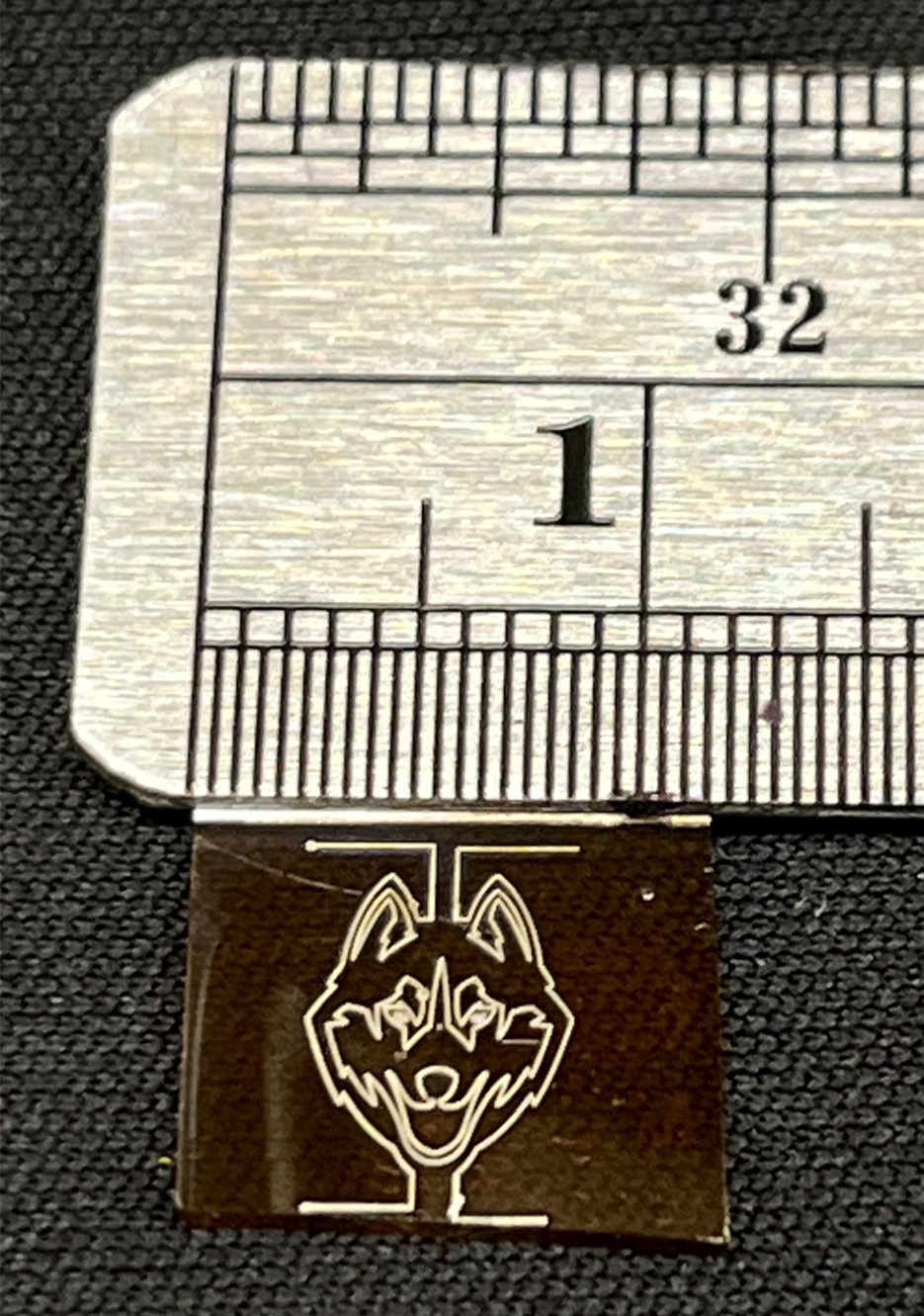
Source: UConn Today, June 3, 2026. Contributed photograph.
01 · 3D Manufacturing
3D Heterogeneous Manufacturing & Embedded Electronics
Writing conductive structures directly inside materials.
Embedding metal pathways within a three-dimensional insulating material creates opportunities for compact devices with more freedom in their geometry. We investigate femtosecond laser direct writing to form conductive silver structures within a gelatin matrix through localized photoreduction.
Published result: conductive embedded circuitry
Our 2025 study demonstrated embedded silver wires, planar patches, and three-dimensional circuitry without additional post-processing, establishing a foundation for integrating conductive features into volumetric materials.
Read the embedded-circuitry paper →
Awasthi & Kang · Materials Today Advances · 2025
3D OHMIC · NSF CAREER
Our NSF CAREER project, 3D One-step Heterogeneous Manufacturing for Integrated Circuits (3D OHMIC), builds on this direction. The project aims to connect precision laser fabrication with high-speed 3D printing and advance the fundamental understanding needed for integrated electronic and photonic structures.

Source: Awasthi, S. & Kang, S. Materials Today Advances 25, 100544 (2025), Fig. 2. DOI / publication.
Reproduced from the figure; article margins and original caption cropped. © 2024 The Authors. CC BY-NC 4.0.
02 · Sensors & Photonics
Laser-Fabricated Sensors & Photonics
Connecting material structure with device response.
Flexible capacitive pressure sensors
We explore how laser-patterned electrodes and microstructures can work together in functional devices. In our flexible capacitive pressure sensor, femtosecond laser writing forms silver electrodes in gelatin, while laser-created microholes increase the pressure response.
We measured repeatable capacitance changes under cyclic loading and demonstrated responses to finger-applied pressure and bending.
Read the flexible pressure-sensor paper →
Palwe, Awasthi, Shukla, Saxena & Kang · Advanced Sensor Research · 2025
Published sensor performance
≈2.44 kPa−1
Sensitivity over 0–0.5 kPa
5 Pa
Reported detection limit

Source: Palwe, A., Awasthi, S., Shukla, S., Saxena, S. & Kang, S. Advanced Sensor Research 4, e00068 (2025), Fig. 6. DOI / publication.
Reproduced from the figure; article margins and original caption cropped. © 2025 The Authors. CC BY 4.0.

Source: Palwe, A. et al. Front Cover. Advanced Sensor Research 5, e70087 (2026). DOI / publication.
Original journal cover reproduced from the supplied cover PDF. Wiley-VCH.
See how the sensor is fabricated

Source: Palwe, A., Awasthi, S., Shukla, S., Saxena, S. & Kang, S. Advanced Sensor Research 4, e00068 (2025), Fig. 1. DOI / publication.
Reproduced from the figure; article margins and original caption cropped. © 2025 The Authors. CC BY 4.0.
Tunable photonic structures
We use three-dimensional finite-difference time-domain (FDTD) simulations to explore tunable spiral-plate designs. The models investigate how geometric compression and refractive-index variation change optical-vortex profiles and focal characteristics.
Explore the spiral-plate study →
Awasthi & Kang · Journal of Physics: Photonics · 2022

Source: Awasthi, S. & Kang, S. Journal of Physics: Photonics 4, 034001 (2022), Figs. 1 and 4. DOI / publication.
Adapted by cropping and arranging source figures. © 2022 The Authors. CC BY 4.0.
03 · Energy Harvesting
Electrochemical Energy Storage & Harvesting
Understanding how mechanical loading changes electrochemical behavior.
Mechanical stress and temperature influence battery response as well as the potential to harvest mechanical energy through piezo-electrochemical (PEC) coupling. We investigate these interactions to understand the tradeoffs between output and stability.
Laser-patterned electrodes for ultra-low-frequency harvesting
Our 2026 iScience study investigates Li-ion battery-based distributed embedded energy converters (DEECs), connecting circuit scaling and material design with PEC harvesting. In proof-of-concept LCO/graphite tests at 10 MPa and 10 µHz, laser-patterned cells harvested 0.50 µJ/cycle versus 0.27 µJ/cycle for non-patterned cells, using separately selected states of charge. Capacity-normalized specific power increased from 16.47 to 37.67 nW/Ah.
Read the 2026 energy-harvesting study →

Source: Aziz, M. A., Khan, A., Karan, N. K. & Kang, S. iScience 29(10), 117319 (2026), Fig. 17. DOI / publication.
Reproduced without alteration to the figure or original caption. © 2026 The Authors. CC BY-NC-ND 4.0.
Battery chemistry, stress & temperature
Our 2025 comparison found a stronger coupling response in lithium cobalt oxide (LCO) under selected conditions, while lithium iron phosphate (LFP) showed greater stability during repeated loading and at low temperatures. These results help inform material selection for PEC energy harvesting.
Aziz & Kang · Electrochimica Acta · 2025
Shared Manufacturing Capabilities
DLP Manufacturing & Mechanical Characterization
Digital light processing (DLP) complements our laser-based research by providing a platform for fabricating and evaluating three-dimensional polymer structures. Our 2026 study introduces a reproducible workflow that combines specimen design, fixture adaptation, and tensile testing to relate print orientation and layer thickness to mechanical response.
Read the DLP design and testing paper →
Awasthi, Balaj, Ni & Kang · The International Journal of Advanced Manufacturing Technology · 2026

Source: Awasthi, S., Balaj, A., Ni, Z. & Kang, S. The International Journal of Advanced Manufacturing Technology 142, 3433–3443 (2026), Fig. 3. DOI / publication.
Reproduced from the figure; article margins and caption cropped. © The Author(s), under exclusive license to Springer-Verlag London Ltd., part of Springer Nature 2026.
Multi-material DLP
Our earlier multi-material DLP work demonstrated embedded carbon-nanocomposite regions and three-dimensional lattice structures, establishing a complementary platform for spatially patterned composite materials.
Read the multi-material DLP paper →
Kang et al. · Journal of Materials Research · 2021
Explore more
Interested in light-enabled manufacturing, functional devices, or materials behavior? Explore our publications and contact the Kang Group to discuss research opportunities and collaboration.